What are Printed Circuit Boards (PCBs)?
_%20-%20.png)
Printed circuit boards (PCBs) are at the core of nearly every modern electronic device. From smartphones and laptops to cars, medical equipment, and industrial machinery, PCBs make today’s technology possible.
At their simplest, PCBs provide a structured way to connect electronic components—such as resistors, capacitors, and chips—through conductive pathways etched into a board. Without them, electronic devices would be bulkier, less reliable, and far harder to manufacture at scale.
In this guide, you’ll learn exactly what a PCB is, why it exists, and how it supports the electronics you rely on every day.
What Is a PCB?

A printed circuit board (PCB), also known as a printed wiring board (PWB) is the foundation of almost every electronic device. It’s a flat board made from an insulating material, usually fiberglass, that provides both structure and connectivity for electronic components.
Instead of wiring each component together manually, PCBs use thin copper pathways—called traces—that are etched or printed onto the surface of the board. These traces create reliable electrical connections between chips, resistors, capacitors, and other components mounted on the board.
What Are PCBs Made Of?
Printed circuit boards are built from layers of different materials, each serving a specific purpose:
- Base/ Substrate: Usually fiberglass-reinforced epoxy resin (FR4).
- Provides mechanical strength and durability.
- Acts as the core structure of the board.
- Provides mechanical strength and durability.
- Copper Layer: A thin layer of copper is laminated onto the substrate.
- Forms the conductive pathways (traces) that connect components.
- Can be single- or multi-layer, depending on circuit complexity.
- Forms the conductive pathways (traces) that connect components.
- Solder Mask: The green (or sometimes blue, red, or black) coating that covers the copper traces.
- Prevents short circuits.
- Protects the copper from oxidation.
- Prevents short circuits.
- Silkscreen Layer: The printed labels (numbers, letters, and symbols) on the PCB surface.
- Helps engineers and assemblers identify parts and test points.
- Helps engineers and assemblers identify parts and test points.
- Finish Materials (optional): For specialized applications, metals such as gold, silver, or tin are applied.
- Improves conductivity, corrosion resistance, and solderability.
- Often used in high-reliability industries like aerospace or medical devices.
- Improves conductivity, corrosion resistance, and solderability.
Industrial Applications of PCBs
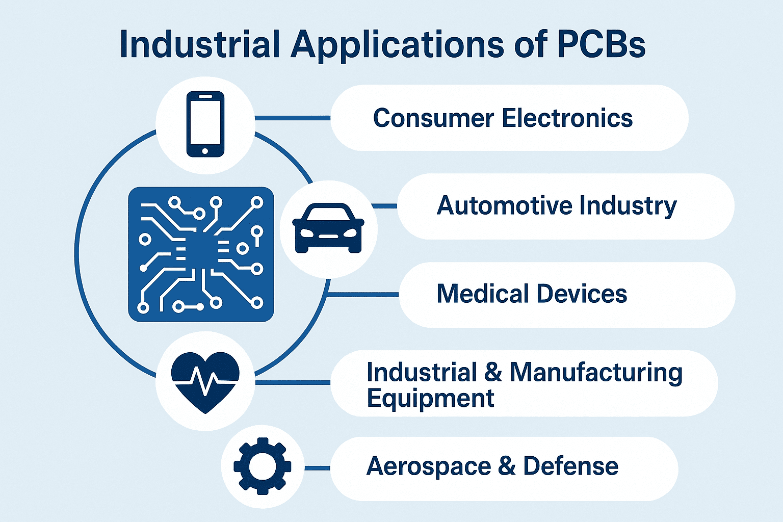
Infographic titled 'Industrial Applications of PCBs' showing five uses: Consumer Electronics, Automotive Industry, Medical Devices, Industrial & Manufacturing Equipment, and Aerospace & Defense, with corresponding icons.
Printed circuit boards are the foundation of nearly every modern electronic system. Their ability to provide reliable interconnections, compact design, and scalable performance makes them essential across a wide range of industries. They are most commonly found in the following:
1. Consumer Electronics
PCBs are the backbone of devices like smartphones, laptops, televisions, and home appliances. They enable compact designs, consistent performance, and integration of multiple functions in one device—making modern electronics both efficient and portable.
2. Automotive Industry
Vehicles today rely on PCBs for advanced driver assistance systems (ADAS), infotainment, power management in electric cars, and safety-critical systems such as airbags and anti-lock braking. Reliability and durability are crucial, as PCBs in vehicles must perform flawlessly under vibration, heat, and varied operating conditions.
3. Medical Devices
From diagnostic tools such as MRI and CT scanners to life-sustaining devices like pacemakers and defibrillators, PCBs are essential for healthcare technology. They must meet strict safety and compliance standards, ensuring precision, reliability, and uninterrupted performance in mission-critical applications.
4. Industrial & Manufacturing Equipment
Automation systems, robotics, and motor controllers depend on rugged PCBs. In these settings, boards must withstand harsh conditions like vibration, dust, and high temperatures, while ensuring long lifecycles and reducing downtime.
5. Aerospace & Defense
PCBs used in aerospace and defense are built to withstand extreme environments, including high vibration, rapid temperature changes, and electromagnetic interference. Applications include avionics, radar, satellite communications, and weapons systems—where reliability and precision are non-negotiable.
How Many Types of PCBs Are There?
There are many types of PCBs, each with their own pros and cons.
- Single-sided PCBs: This is the most common type of PCB, as it requires fewer steps in manufacturing than double sided boards. It also allows you to use simpler components on one side and more complex ones on the other side without having to worry about things like component placement or trace routing. The only downside here is that this type of board has limited usage since there isn't much room for components between two sides (and if there are multiple layers).
- Double-sided PCBs: Since both sides have tracks running across them, these kinds of boards can be used for more complicated projects with larger amounts of circuitry or multiple chipsets in one unit (like WiFi routers). However, these kinds of boards take longer to make because they require up to six layers instead of four like single-sided models do.
- Multi Layer PCBs : These types usually have extra traces running vertically along both edges making them more durable but costing more money.
Other types of PCBs include:
- Rigid PCBs: These are most commonly used in computers. They can be made from a variety of materials including copper foil laminate or fiberglass epoxy resin with copper foil traces on its surface.
- Flexi PCBs: This type is used mainly on electronic devices with small dimensions that need flexibility in their design (like wearables). Flexi is short for flexible PCB.
- Metal core PCBs: These boards use aluminum as the base instead of traditional FR4.
- Ceramic PCBs: Ceramic is often used as the base material in these types of boards because it has better thermal conductivity and resistance to high temperatures than fiberglass epoxy resin (FR4). This makes them ideal for use in high-power electronics applications where heat dissipation is an issue.
PCB Design and Manufacture
Designing and manufacturing printed circuit boards are two connected stages of the same process. The design defines how the board will function, while manufacturing turns that design into a physical product.
PCB Design
PCB design focuses on planning the layout of the board to meet the needs of the electronic device. This step involves:
- Creating a schematic diagram to represent the circuit.
- Placing components (resistors, capacitors, ICs) on the board.
- Routing traces to connect the components.
- Adding power planes, solder mask, and silkscreen labels for assembly and identification.
A good PCB design ensures:
- Efficiency and reliability.
- Compliance with electrical and mechanical requirements.
- Ease of manufacturing without costly rework.
PCB Manufacturing
Once the design is ready, the board moves into production. Key steps in PCB manufacturing include:
- Selecting the right substrate materials (commonly fiberglass-reinforced epoxy).
- Applying copper layers to form conductive pathways.
- Using photolithography or other methods to create circuit patterns.
- Etching away excess copper.
- Drilling holes for mounting and connections.
- Applying solder mask and silkscreen markings.
Design and Manufacturing Link
The quality of a PCB depends on how well the design accounts for manufacturing constraints. Designers must factor in:
- Minimum trace widths and spacing.
- Drill size limitations.
- Proper placement of components for manufacturability.
PCBA vs. PCB
Printed Circuit Board Assembly (PCBA) refers to the process of populating a printed circuit board (PCB) with electronic components and soldering them to the PCB to create a functional electronic assembly. PCBA is a critical step in the manufacturing of electronic products, as it involves placing and soldering various electronic components onto the PCB to create a complete and functional circuit.
The PCBA process typically involves the following steps:
- Component Placement: Electronic components, such as resistors, capacitors, diodes, transistors, and integrated circuits (ICs), are placed onto the PCB according to the component placement information provided in the PCB design. This can be done manually or using automated pick-and-place machines, depending on the volume and complexity of the assembly.
- Solder Paste Application: Solder paste, a mixture of solder alloy and flux, is applied to the PCB's solder pads. The solder paste serves as the medium for attaching the components to the PCB during the soldering process.
- Soldering: The PCB with the components and solder paste is subjected to a soldering process, typically involving reflow soldering or wave soldering. In reflow soldering, the PCB is heated in a controlled manner to melt the solder paste and create solder joints that bond the components to the PCB. In wave soldering, the PCB is passed over a wave of molten solder, which selectively solders the components to the PCB.
- Inspection and Testing: After soldering, the PCBA is inspected for proper solder joint quality, component alignment, and other visual defects. Functional testing may also be performed to ensure that the assembled PCB functions as intended.
- Post-Assembly Processes: Depending on the specific requirements of the product, post-assembly processes such as cleaning, conformal coating, and encapsulation may be performed to further protect and enhance the reliability of the PCBA.
Once the PCBA process is complete and the assembled PCB passes inspection and testing, it can be integrated into the final electronic product, such as a computer, smartphone, medical device, or any other electronic system.
Where to Source PCBs

Once you understand what PCBs are and how they’re manufactured, the next step is knowing where to source them. Depending on your needs—small batches for prototyping or large volumes for industrial production—different sourcing channels may be appropriate.
1. Authorized Distributors and Online Marketplaces
For standard, new production PCBs, most companies rely on well-known distributors and marketplaces. Online platforms provide access to a diverse range of PCB boards, materials, and assemblies. These channels are reliable for sourcing directly from manufacturers, ensuring quality and traceability.
2. Direct from Manufacturers
Large enterprises or those with specialized requirements often source PCBs directly from original manufacturers. This approach is useful when ordering in bulk, working with custom PCB designs, or when requiring strict compliance with certifications and testing standards. Direct sourcing typically involves higher minimum order quantities and longer lead times.
3. Brokers and Search Engines
When you’re looking for less common PCBs or specific configurations, component brokers and search engines can help locate available stock across global suppliers. However, this path requires careful vetting, as quality and authenticity can vary.
4. Liquidation-Based Procurement
An often-overlooked sourcing option is liquidation-based procurement. This involves buying unused, surplus, or discontinued PCBs from industrial sellers via different industrial liquidation channels.
This channel provides clear advantages:
- Cost savings compared to new production or distributor pricing.
- Access to hard-to-find or obsolete PCBs that are often unavailable through traditional suppliers, helping overcome component obsolescence.
- Sustainability benefits, since surplus boards are put back into use rather than scrapped.
Note: The key is working with reputable liquidators who provide proper documentation and quality assurance.
Source PCBs Smarter with Amplio
Amplio’s online platform connects you directly with a network of vetted industrial sellers offering surplus and excess PCBs.
With Amplio, you can:
- Access hard-to-find boards that may be unavailable through standard suppliers.
- Reduce procurement costs by sourcing from liquidation-based listings.
- Work with our support team to locate the exact PCB specifications you need, without wasting time across multiple vendors.
Contact us today and see how our platform simplifies PCB sourcing while giving you more control over cost and availability.